![]()
Manufacturing a computer chip is a complex process involving hundreds of steps and requiring from a few days to up to three months of processing time to complete. Chip making demands incredible precision, careful attention to detail, and constant testing.
IBM is a leader in chip manufacturing, and has invested extensively in its world-class facilities to be able to produce some of the most advanced memory, logic, and microprocessor chips in the industry.
Silicon is the crucial building block in the fabrication of computer chips. Raw silicon is first extracted from common sand. A series of chemical steps refine it until the purity level reaches 99.9999999 percent. Thus, for every ten billion atoms, only one non-silicon atom can be permitted. That is like one tennis ball in a line of ping pong balls stretching from the earth to the moon.
Silicon ingots are then "grown" from the purified molten silicon and sliced
into round wafers ranging from 150mm to 200mm
(6 to 8 inches) in diameter with a thickness about that of a credit card.
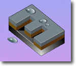
 The structure of
a computer chip is complex, both on its surface and in its internal three-dimensional
composition. The chip is made up of many layers, each of which is a detailed pattern. Some
of the layers lie within the silicon wafer and others are stacked on top. The
manufacturing process consists of forming this sequence of layers very precisely.
The structure of
a computer chip is complex, both on its surface and in its internal three-dimensional
composition. The chip is made up of many layers, each of which is a detailed pattern. Some
of the layers lie within the silicon wafer and others are stacked on top. The
manufacturing process consists of forming this sequence of layers very precisely.
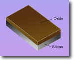
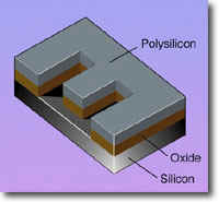
 For example, a thin layer of silicon
dioxide, an insulating material, may be "grown" on the surface of the wafers.
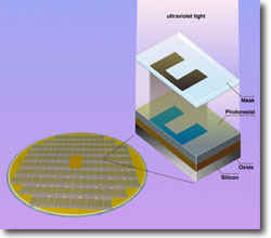
Microscopically small circuits, some 250 times smaller than a human hair, are then built
on this and successive layers of silicon dioxide. Microminiature areas on these wafers can
then be turned into electrical conductors by adding minute amounts of impurities, known as
dopants, at selected areas in these detailed patterns.
For example, a thin layer of silicon
dioxide, an insulating material, may be "grown" on the surface of the wafers.
Microscopically small circuits, some 250 times smaller than a human hair, are then built
on this and successive layers of silicon dioxide. Microminiature areas on these wafers can
then be turned into electrical conductors by adding minute amounts of impurities, known as
dopants, at selected areas in these detailed patterns.
 The unexposed photoresist is washed away
in solvent baths, etching the protective oxide layer with the shape of the circuit
patterns. Tiny holes are then etched into the oxide layer in preparation for the next
major process step.
The unexposed photoresist is washed away
in solvent baths, etching the protective oxide layer with the shape of the circuit
patterns. Tiny holes are then etched into the oxide layer in preparation for the next
major process step.
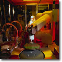
Although a photolithographic process is used to print the circuit patterns on the chip,
this process is millions of times more precise than the process used by the printing
industry. This and other operations are performed by computer-controlled robotic devices
in "clean rooms" that are a thousand times cleaner than a hospital operating
room. No human hand is ever allowed to touch a wafer. Workers are garbed in "bunny
suits" that cover them from head to toe. The air is continuously filtered and
recirculated to keep the dust level at an absolute minimum. 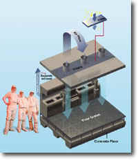 Temperature, barometric pressure, and humidity are
controlled to unheard of tolerances in order to protect microscopic circuits that, in some
advanced IBM technologies, measure slightly more than a polio virus. In fact, a single
particle of smoke, if it were allowed to infiltrate a semiconductor "white
room," could destroy an entire chip.
Temperature, barometric pressure, and humidity are
controlled to unheard of tolerances in order to protect microscopic circuits that, in some
advanced IBM technologies, measure slightly more than a polio virus. In fact, a single
particle of smoke, if it were allowed to infiltrate a semiconductor "white
room," could destroy an entire chip.
After the circuit patterns have been printed, the wafer is then
"doped" with more impurity atoms, such as boron or phosphorus, to form positive
and negative conducting regions. The dopant atoms are ionized (stripped of one or more of
their electrons) and accelerated to a high energy in ion implantation chambers. The ions
bombard the silicon wafer and penetrate the holes etched in the protective oxide layer.
The depth and concentration of these impurities determine the specific
electrical
characteristics of the chip. 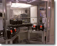
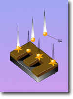
The processes of oxidation, photolithography, etching, and ion implantation are repeated many times to build the transistors and other electronic circuitry that make up each chip on a wafer.
Once the electronic components have been fabricated in the silicon, thin metallic and doped polysilicon films are added to form the interconnections among individual transistors and other devices. On some IBM logic chips, there may be up to six layers of these minute interconnecting wires joining together over four million circuits. A protective coating of polysilicon is then deposited on the wafers to protect the chips from moisture, corrosion, and atmospheric contamination.
Low-angle scanning electron micrograph of a portion of a partially completed SRAM array containing six-device memory cells. The insulating oxide films have been removed, revealing the lower levels of the interconnection structure of the array.
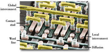
The word lines (colored green) are salicided polysilicon lines (running horizontally). The local interconnections (tungsten; colored pink) provide cross-coupling for the n+ and p+ diffusion contacts and act as the lower portions of the contact studs to the first global interconnection level Ti/A1(Cu)/Ti/TiN; (colored yellow). The contact studs (tungsten; colored grey) constitute the upper portions of the contact paths to the global interconnections.
At each step of the process, wafers are tested with specially designed equipment under computer control, some of which measure events on an atomic scale. When the metalization process is completed, all the chips on a wafer are tested again. Those that pass the rigorous electrical tests are then cut from the wafer with high-speed, water-cooled diamond cutting saws and mounted in metal or plastic packages, called modules. These modules are then tested again.
Each tiny memory cell that holds a bit of information, and every circuit must be tested. Since only one of IBM's advanced eight-inch memory wafers contain as many memory cells as there are people on earth, it takes extraordinary care and precision to produce reliable chips.

![]()
Click here if you do not see navigation menu on your left.
This information is © International Business Machines. The original page can be reached here.